Datasheet4U Logo Datasheet4U.com

V54C365164VL - 3.3 VOLT 4M X 16 SYNCHRONOUS DRAM

Download the V54C365164VL datasheet PDF. This datasheet also covers the V54C365164VD variant, as both devices belong to the same 3.3 volt 4m x 16 synchronous dram family and are provided as variant models within a single manufacturer datasheet.

General Description

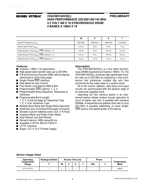
The V54C365164VD(L) is a four bank Synchronous DRAM organized as 4 banks x 1Mbit x 16.

Key Features

  • s 4 banks x 1Mbit x 16 organization s High speed data transfer rates up to 225 MHz s Full Synchronous Dynamic RAM, with all signals referenced to clock rising edge s Single Pulsed RAS Interface s Data Mask for byte Control s Four Banks controlled by BA0 & BA1 s Programmable CAS Latency: 1, 2, 3 s Programmable Wrap Sequence: Sequential or Interleave s Programmable Burst Length: 1, 2, 4, 8 and full page for Sequential Type 1, 2, 4, 8 for Interleave Type s Multiple Burst Read with Single Write Oper.

📥 Download Datasheet

Note: The manufacturer provides a single datasheet file (V54C365164VD_MoselVitelic.pdf) that lists specifications for multiple related part numbers.

Datasheet Details

Part number V54C365164VL
Manufacturer Mosel Vitelic
File Size 0.97 MB
Description 3.3 VOLT 4M X 16 SYNCHRONOUS DRAM
Datasheet download datasheet V54C365164VL Datasheet

Full PDF Text Transcription (Reference)

The following content is an automatically extracted verbatim text from the original manufacturer datasheet and is provided for reference purposes only.

View original datasheet text
w w w . D a t a S h e e t 4 U . c o m MOSEL VITELIC V54C365164VD(L) HIGH PERFORMANCE 225/200/166/143 MHz 3.3 VOLT 4M X 16 SYNCHRONOUS DRAM 4 BANKS X 1Mbit X 16 PRELIMINARY 45 System Frequency (fCK) Clock Cycle Time (tCK3) Clock Access Time (tAC3) CAS Latency = 3 Clock Access Time (tAC2) CAS Latency = 2 Clock Access Time (tAC1) CAS Latency = 1 225 MHz 4.5 ns 4.5 ns 4.5 ns 12 ns 5 200 MHz 5 ns 5 ns 5 ns 12 ns 6 166 MHz 6 ns 5.4 ns 5.5 ns 12 ns 7 143 MHz 7 ns 5.4 ns 5.